
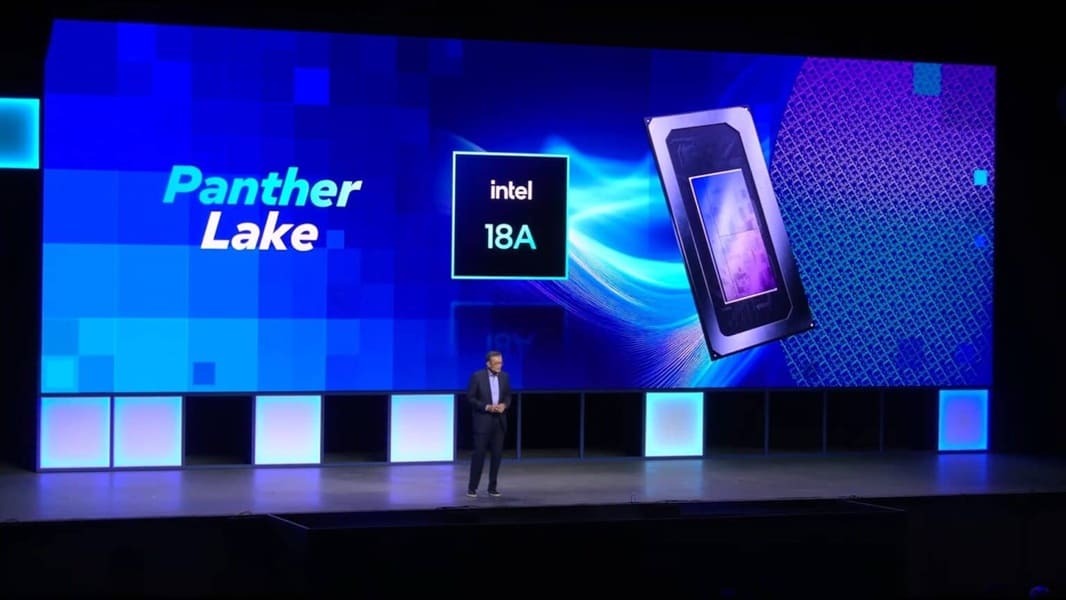
The Intel 18A and Panther Lake Paradigm Shift
It is a defining moment for Intel to be able to showcase that it is at the forefront of semiconductor manufacturing again. Innovations like the next-generation client processor, Panther Lake (first known as the Intel Core Ultra series 3), could be envisaged as a clear move in that direction, signifying a new era. The Intel 18A process technology at the 1.8-nanometer-class node is the technology that the chip is to spearhead.
Such a step embarks on the company’s ambitious plan to revive the “five nodes in four years” strategy. The timeline is quite extraordinary, with the debut of the first client devices bearing the Panther Lake architecture scheduled for January 2026.
While the client platform unveiling is the new server platform’s (Clearwater Forest (Xeon 6+)) counterpart, the duo are tightly coupled. Clearwater Forest will likewise feature the 18A process and is slated for the first half of 2026. Close dependency of this kind is a double risk. Any setback in the 18A HVM schedule can potentially close the doors to not only the enormous laptop market of the consumer sector but also the lucrative data center segment. In other words, impeccable operational performance should be on par with this technological leap.
Ramping up performance Intel’s 18A process technology
The Intel 18A process technology features two first-in-the-world production technologies. These breakthroughs are vital to breaking through the physical barriers of sub-2 nm production.
RibbonFET: The Gate-All-Around Transition
Fundamental to 18A is RibbonFET, Intel’s radical new transistor design with Gate-All-Around (GAA) architecture. It is the first time that in more than ten years Intel has drastically changed the transistor architecture. The FinFET design, which the new one is replacing, has already hit its scaling limits at the Angstrom level.
RibbonFET utilizes several horizontal nanowire ribbons that are fully enclosed by the gate material. As a result, both the density and transistor performance are substantially enhanced. Additionally, the refined system also pumps out more performance for every watt consumed, which is very important for energy savings in end products like Panther Lake.
PowerVia: Backside Power Delivery Network (BSPDN)
The 18A process is perhaps most famously characterized by its PowerVia, the world’s first Backside Power Delivery Network (BSPDN). With this innovative network, the issues of power integrity that come with densely packed chip design are resolved.
The main idea behind PowerVia is that the power delivery lines are detached from the front side of the wafer and put on the backside. In this way, they are brought into the proximity of the ground and power reference planes and hence isolated from the signal lines, which are left on the front side. This kind of architectural decoupling exhibits quite a few good things. It results in an uplift of 5% to 10% in cell utilization and a rise in performance at ISO power by as much as 4%.
Apart from that, the disconnection leads to less noise and more stable power rails. It is this stability that allows the chip to be run at elevated frequencies and at lower voltages while still maintaining its reliability. Modern workloads, which are typically characterized by a high load, such as generative AI, can benefit a lot from this feature, and in fact, it is one of the direct reasons for 18A’s enhanced logic performance.
At the same time, generative improvements of the same magnitude are achieved by the coupling of RibbonFET and PowerVia. Thus, Intel announces that the 18A node can deliver as much as 15% better performance per watt as well as 30% greater chip density with respect to the technologically closest competitor, the Intel 3 node.
Architecting the AI PC: Panther Lake’s XPU Strategy
The power efficiency and scalability of performance were the primary concerns behind the design of the client chip, Panther Lake, based on 18A. It is equipped with up to 16 new P-cores and E-cores. The radical power efficiency gains are the architect of the system.
Power Efficiency and Core Design
By pairing core designs that have been freshened up with the 18A features, one can achieve the enormous feat of cutting the power use by 40% of the single-threaded workloads and thus maintaining the level of performance. For multi-threaded applications, in the same power envelope setting, Panther Lake can increase the output of performance by as much as 50%.
To achieve “always-on” capability with a low-power battery, Panther Lake is equipped with a Low-Power Efficiency (LPE) cluster of four E-cores. These cores are made to maintain the power efficiency level of Lunar Lake, which makes them very suitable for handling background and idle tasks. The emphasis on energy efficiency is what helps the company to close the competitive gap with ARM-based opponents that are high in efficiency.
The AI PC Imperative: XPU Acceleration
Panther Lake is an XPU (CPU + GPU + NPU) platform optimized for the AI PC segment that is the future of the market. The entire platform can deliver up to 180 trillion operations per second (TOPS) for AI acceleration.
Intel’s game plan is to get the most out of the graphics engine to maximize throughput. The new Xe 3 graphics architecture is, by far, the most powerful AI engine, and it is capable of producing a massive 120 TOPS for AI tasks. A small increase to 50 TOPS is what the Neural Processing Unit (NPU) is witnessing. This is a clear indication that the majority of the high-throughput processing for large visual models and local Large Language Models (LLMs) is being transferred to the strong integrated GPU.
Intel leads with a 12% performance advantage for a representative mix of AI visual inference workloads and shows a corresponding power advantage. The peak FP32 GPU power at 2.9 GHz drops from 185W for Raptor Lake to 125W for Panther Lake. This is a reason behind the power efficiency of the new system.
Competitive Edge and Market Trade-Offs
The “foundry war” between Intel and TSMC is one where the tech specs of Intel 18A and TSMC N2 reveal a throttling trade-off affecting the performance of both chips.
18A vs. TSMC N2 Foundry War
First of all, in terms of power and performance stability, the advantage seems to be on the Intel 18A side, and that is largely because of its earlier use of PowerVia (BSPDN). As for TSMC, they are holding BSPDN back until their A16 node.
Comparatively, Intel’s 18A technology seems to beat TSMC’s N2 with improvements in performance and power stability. The main reason for this is the very early implementation of PowerVia (BSPDN) on Intel 18A. On the other hand, TSMC is postponing BSPDN to its A16 node.
On the other hand, TSMC’s 2 nm process clearly outperforms Intel’s 18A in terms of chip density and SRAM scaling. In terms of chip density, TSMC’s 2 nm process is around 313 million transistors per square millimeter (MTx/mm²), while Intel’s 18A is about 238 MTx/mm². It seems that with this selection of features, Intel 18A is best suited for maximum speed, power stability, and high-performance logic, which goes well with crazily large chips like Clearwater Forest.
Client CPU Rivalry
Mobile market-wise, Panther Lake has to contend with the longtime rival AMD and the growing ARM ecosystem (Qualcomm Snapdragon X Elite).
While competing with AMD, Panther Lake is empowered with a high core count and the strong, next-generation Xe3 integrated GPU. To make the mobile architecture more power-efficient, Intel is simplifying it on the 18A node by, for instance, omission of SMT (Hyperthreading) and the full 512-bit side of AVX10.
The confrontation ARM, Panther Lake’s architectural design, can be seen mainly as a defensible one. The 40% power reduction factor is quite a clear indication that they want to close the power efficiency gap by introducing the LPE cluster. By reaching high efficiency while still providing the performance and software compatibility of the x86 platform, Panther Lake would be able to deliver equal battery life for normal user scenarios.
The Critical IDM 2.0 Execution Risk
The successful utilization of the 18A process technology depends a lot on the ramp-up of operations at Fab 52 in Arizona, which is a $20 billion investment and a major Intel IDM 2.0 strategy component.
Fab 52 and Clearwater Forest Synchronization
The lead risk in the 18A HVM ramp-up execution at Fab 52 is the defining moment. The 18A process is the base for the server segment’s big release, Clearwater Forest (Xeon 6+). This server chip is a gargantuan, sophisticated die made for hyperscale data centers, and it can have up to 288 E-cores.
Launching simultaneously the high-volume Panther Lake and the complicated Clearwater Forest on the same node results in an extraordinary demand for yield stability. Because of the big die of Clearwater Forest, even a slight defect in the 18A process will drastically reduce the number of server chips of good quality. Intel’s single most important operational metric in terms of the company’s credibility and revenue over 2026 is how fast 18A yields can be stabilized.
Financial Reality and Investor Perception
The advanced technological capabilities stand juxtaposed to Intel’s continuing financial struggles that include net losses and costly restructuring activities. The market’s reaction to the technological reveal was not what was expected – it resulted in a stock price drop.
This underlines the continued skepticism of investors that mainly consider the high risk of execution and the enormous capital expenditure as the biggest obstacles. The financial turnaround depends mainly on the Intel Foundry unit being able to break even by 2027. Achieving this target necessitates a vast external customer base and faultless execution of the 18A ramp-up, thereby demonstrating that a technological lead can result in sustainable high-volume profitability.
Conclusion
The use of the Intel 18A process technology for Panther Lake is an impressive technological breakthrough. The 18A node which is the first in the industry to use PowerVia (BSPDN) and RibbonFET (GAA) (both 2nm class) structures is at the forefront in terms of both performance and power stability. The client CPU performance is thus made more than 50% faster and at the same time, a groundbreaking 180 Platform TOPS for local AI acceleration is achieved.
With the aggressive addressing the power efficiency challenge posed by ARM-based competitors, Intel has cleverly designed Panther Lake to be the x86 platform’s mainstay. Besides, the coordination of the client (Panther Lake) and server (Clearwater Forest) roadmaps on 18A is an effective way of operational leverage of the new node.
The technology is confirmed and top-notch, but the way forward is not straightforward. The whole IDM 2.0 strategy depends heavily on the 18A node high-volume yield at Fab 52 that it has to be both timely and consistent. To beat the financial challenges and market skepticism, the operations have to be successful at the level of the technology very soon. Whether Intel will be able to use the 18A/Panther Lake platform as a springboard for her long-term comeback will be mostly a function of how well she can stabilize yields and therefore, as a result of that, attract external foundry customers.